Office Address
S.C Chatterjee Road - Bandel
Prantik Benepukir
IN - West Bengal
Hooghly - 712123
Lightout, Gunsout, Wingsout, Fansout, AMD Patent’s and interesting GPU Design to GLUE stuff even more.
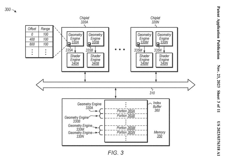
AMD has filed a patent for a new GPU design called Distributed Geometry. This design would distribute the rendering workload across multiple chiplets, rather than having one large die handle all of the processing. This approach could provide several benefits, including improved performance and scalability. This new information came from our Dear Paul at RedGamingTech.
In current GPUs, there is a central workload processor that sends out rendering tasks to one of the many blocks of shaders within the chip. This approach has been used for decades, and both AMD and Nvidia have refined it to a high degree.
However, AMD’s new patent proposes a different approach. Instead of having a central workload processor, the chip would be divided into multiple chiplets, each of which would handle its rendering tasks. This would allow for a more distributed workload, which could improve performance.
In addition, the chiplet approach would be more scalable. As the number of chiplets increases, the rendering workload can be spread across more cores, which can further improve performance.
It is unclear when AMD will release a GPU based on the Distributed Geometry patent. However, this new design could represent a significant step forward in GPU technology.
AMD’s new patent for a new GPU design called Distributed Geometry would distribute the rendering workload across multiple chiplets, rather than having one large die handle all of the processing. This approach could provide several benefits, including improved performance and scalability.
Reduced Manufacturing Costs
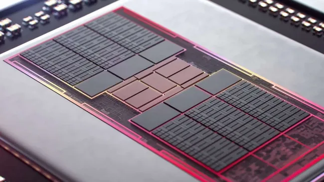
As we’ve seen from AMD’s successful switch to chiplets for its CPUs, it’s mostly about reducing manufacturing costs for high-end hardware. Very large GPUs are less cost-effective to make than smaller ones because each silicon wafer yields fewer working dies. The memory chiplets in the Navi 31 are so small that a typical 12-inch wafer can churn out over a thousand of them, and even if a large number of them are defective, you’ve still got a small mountain of working chips.
AMD clearly wants to take the same approach with the rest of the GPU. Cutting-edge process nodes are hugely expensive so if a high-end GPU can be made by simply putting a stack of tiny chiplets together in the same package, the overall cost of making it can be reduced. Honestly, this would end up being a Ryzen moment vs Intel, just against the greedy green Nvidia. Oh how it gives joy to think about a future where a flagship XTX or any other XYZ starts from $699 (good old 1080 Ti days)
Improved Performance and Scalability
In addition, the chiplet approach would be more scalable. As the number of chiplets increases, the rendering workload can be spread across more cores, which can further improve performance
In addition to the bandwidth and latency challenges, there are other potential issues that AMD will need to address in order to make distributed geometry a viable design for GPUs, and I have done a rundown of issues I think could be present from the RDNA 3 Architecture.
On second thought, there are serious challenges that need to be overcome for this to be an effective way of building a GPU. The first of which is the internal bandwidth and latency requirements. Inside a normal graphics processor, you can have multiple terabytes of data being read and written between the caches each second, taking just a few nanoseconds for each transaction to take place. By switching to chipsets, the system used to connect everything to the shared cache and memory controllers needs to be seriously hardcore.
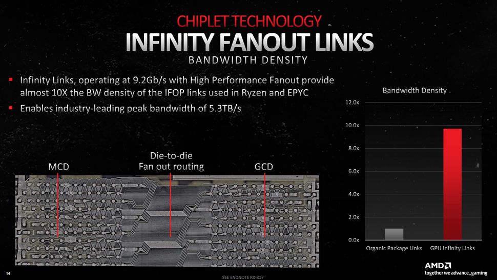
Fortunately, AMD already has plenty of experience in this situation. The Infinity Fanout Links used in the RX 7900 series, to connect the GCD to the memory chips, supply masses of bandwidth and the latency isn’t that much worse than that seen in a full-die GPU, such as the Navi 21 (RX 6900 XT). What would be needed for this distributed geometry design is a fair step up from this, but if anyone can figure it out, it’s going to be AMD.
Workload Balancing
One challenge is ensuring that all of the chiplets are kept as busy as possible. With each chiplet determining its workload, there’s a risk that some units will be left idle because others can work through what’s needed quickly enough. This could lead to wasted resources and reduced performance.
Processing Stalls
Another challenge is processing stalls, where a chiplet can’t fully complete a task because it requires neighboring geometry information. This could happen if the geometry is stored on a different chiplet, or if it’s not yet been fully processed by the previous chiplet in the pipeline.
AMD’s patent doesn’t discuss how these challenges would be addressed, so for now, it’s unclear how the company plans to overcome them. However, AMD has a history of innovation in GPU design, and they likely have some creative solutions in the works.
Timeline
It’s also unclear when AMD might release a GPU based on the distributed geometry patent. The patent was filed in April 2023, and it typically takes about two years for a patent to be granted. However, it’s possible that AMD could release a product based on the technology before the patent is granted.
Some rumors suggest that distributed geometry could be used in RDNA 4, which is expected to be released in 2024. However, other rumors suggest that AMD is focusing on its mainstream portfolio for 2024 and that distributed geometry could be pushed back to 2025 or even 2026.