Office Address
S.C Chatterjee Road - Bandel
Prantik Benepukir
IN - West Bengal
Hooghly - 712123
Intel asserts its 3D stacked CMOS transtiors, which combine direct backside contact and backside power to provide increased performance and scaling for next-generation chips, are a better way to glue things together.
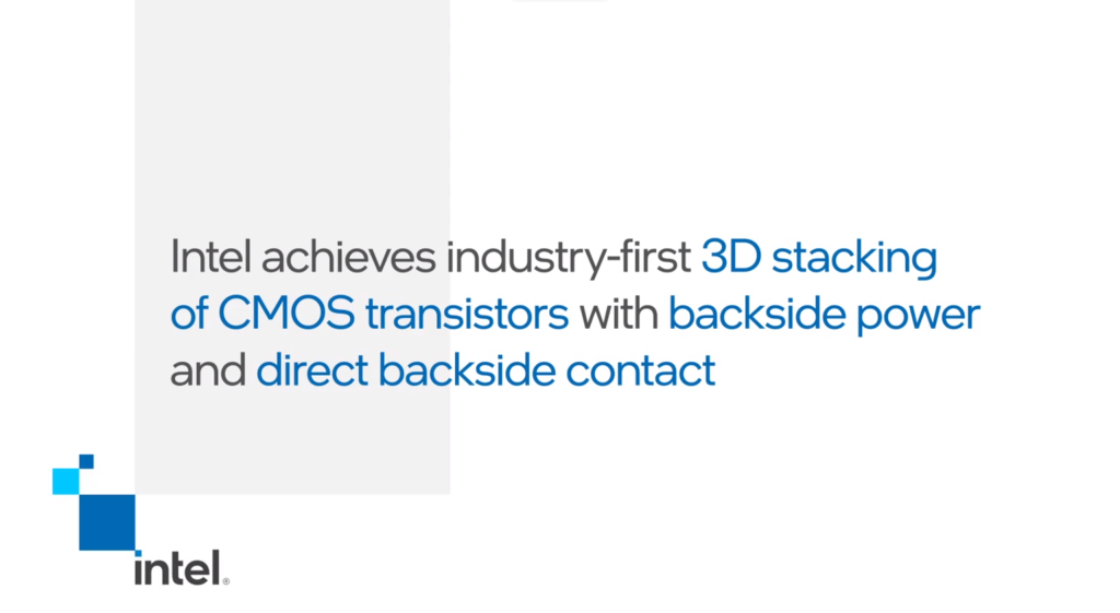
In semiconductors, continuous innovation is the key to pushing the boundaries of Moore’s Law. One such innovation that has caught the tech world’s attention is Intel’s 3D Stacked Complementary Metal-Oxide-Semiconductor (CMOS) transistors.
In semiconductors, continuous gluing things/coughs (innovation) is the key to pushing the boundaries of Moore’s Law. One such innovation that has caught the attention of the tech world is Intel’s 3D Stacked Complementary Metal-Oxide-Semiconductor (CMOS) transistors
“As we enter the Angstrom Era and look beyond five nodes in four years, continued innovation is more critical than ever. At IEDM 2023, Intel showcases its progress with research advancements that fuel Moore’s Law, underscoring our ability to bring leading-edge technologies that enable further scaling and efficient power delivery for the next generation of mobile computing.”
Sanjay Natarajan, Intel senior vice president and general manager of Components Research
Intel researchers demonstrated advances in 3D stacked complementary metal oxide semiconductor (CMOS) transistors with backside power and direct backside contacts at the 2023 IEEE International Electron Devices Meeting (IEDM). The company was the first to demonstrate successful large-scale 3D monolithic integration of silicon transistors with gallium nitride (GaN) transistors on the same 300-millimeter (mm) wafer, rather than on the package. It also reported on scaling paths for recent R&D breakthroughs for backside power delivery, such as backside contacts.
Why This Is Important: Well firstly, it’s intel so it’s not gluing things, and secondly, to help meet the exponentially growing demand for more powerful computing, transistor scaling, and backside power are essential. Every year, Intel satisfies this demand for computing power, proving that its innovations will keep driving the semiconductor industry and serve as the foundation for Moore’s Law. By stacking transistors, increasing backside power to allow for more transistor scaling and better performance, and proving that transistors made of different materials can be integrated on the same wafer, Intel’s Components Research group continuously pushes the limits of engineering.

Intel provides 3D stacked CMOS transistors with backside power and backside contact, a first for the industry:
An industry first was demonstrated by Intel’s most recent transistor research, which was presented at IEDM 2023: the capacity to vertically stack complementary field effect transistors (CFET) at a scaled gate pitch as small as 60 nanometers (nm). This makes stacking transistors possible, which improves performance and area efficiency. Direct backside contacts and backside power are also combined with it. It highlights Intel’s superiority over rivals in the field of gate-all-around transistors and demonstrates the company’s capacity for innovation beyond RibbonFET.

Intel identifies critical research and development domains required to sustain transistor scaling with backside power delivery, surpassing five nodes in four years:
2024 will see the first commercial release of Intel’s PowerVia, the first backside power delivery system. Components Research revealed at IEDM 2023 the critical process advancements needed to enable backside power delivery paths that go beyond PowerVia. Furthermore, this work demonstrated how to enable area-efficient device stacking by utilizing backside contacts and other cutting-edge vertical interconnects.


