Office Address
S.C Chatterjee Road - Bandel
Prantik Benepukir
IN - West Bengal
Hooghly - 712123
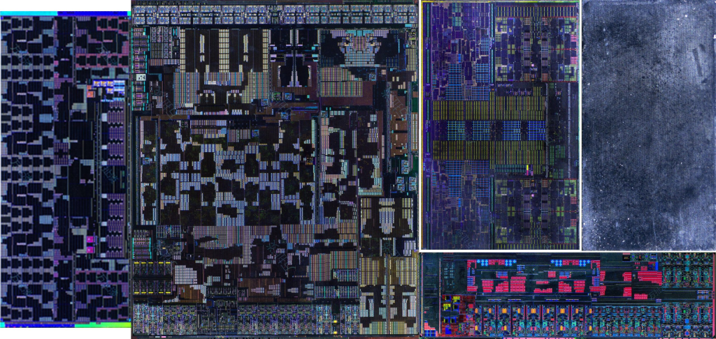
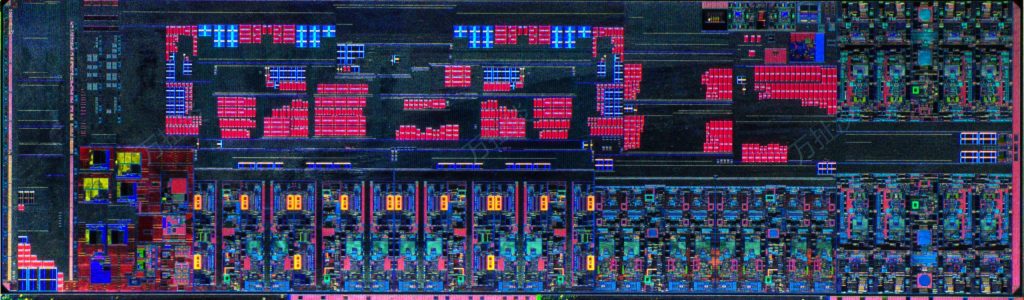
The Intel Core Ultra “Meteor Lake” CPUs have received their first die shots, providing a closer look at the different IPs incorporated. The die shots were posted by HXL (@9559pro) and offer a better understanding of the chiplet (Tile) layout of the Meteor Lake CPUs.
Source: WCCF Tech
The Intel Core Ultra “Meteor Lake” CPUs are based on a disaggregated architecture that combines various IPs on a singular package in a chipset-esque fashion. For Meteor Lake, there are a total of four chiplets which include a Compute (CPU), Graphics (GPU), SOC (NPU, etc), and I/O tiles.
All four tiles will utilize internal and external fabrication processes. This means that some of the tiles will be made by Intel while the rest will be made by 3rd party fabs such as TSMC. The main CPU tile will be using the “Intel 4” or 7nm EUV process node while the SOC Tile and IOE Tiles will be fabricated on TSMC’s 6nm process node (N6).
The tGPU, a new name for the iGPU (Tiled-GPU), is also a major component of Meteor Lake CPUs and utilizes TSMC’s 5nm process node. The die-shots were taken from a 2+8+2 SKU which includes 2 P-Cores based on the Redwood Cove, 8 E-Cores based on the Crestmont, and 2 additional but low-power E-Cores based on the very same Crestmont E-Cores. The first 2 P-Cores and 8 E-Cores reside within the Compute (CPU) tile.
In the case of this configuration, there is a total of 12 MB of Smart Cache with the Redwood Cove P-Cores featuring 2 MB L2 per core, and the Crestmont E-Cores pack 4 MB of L2 cache per cluster.
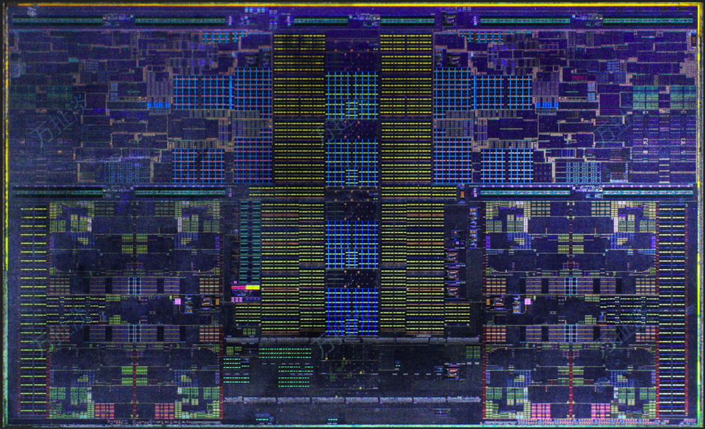
Moving over the GPU tile, we have a 4 Xe-Core variant based on the Arc Alchemist architecture. The most jam-packaged sections seem to be the SOC and I/O tile which have various parts such as controllers (Memory/Storage/PCIe), NPUs, a dedicated low-power island for Video & a lot more. The SOC tile has two Crestmont LP E-Cores.
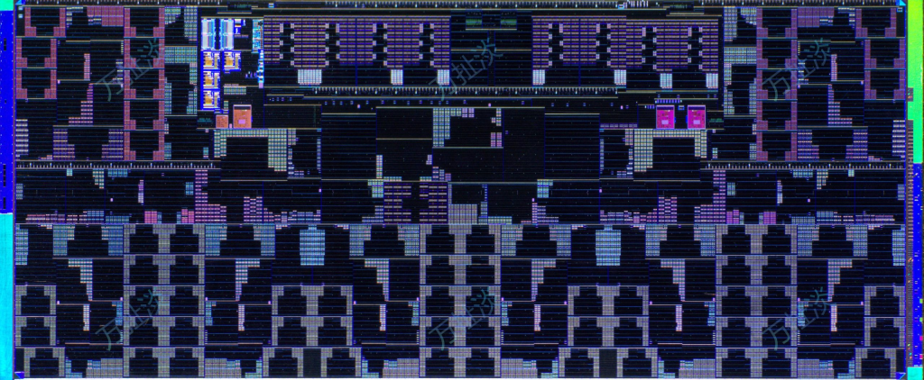
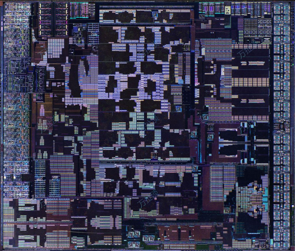
In addition to the detailed die shots of the Intel Core Ultra “Meteor Lake” CPUs, there’s also a dummy spacer die in the configuration. This dummy spacer die was also featured in the recently unveiled Thermal Test Dies for the same CPUs. The die was specifically designed to conduct thermal envelope tests for both 2+8 and 6+8 SKU configurations.
Source:(HXL via QQ)
Interestingly, if you look closely, you’ll notice that the 2+8 dies have almost half the area empty.
Based on the information available on WCCF Tech website, as per analysis from OneRaichu & Andreas Schilling, the die size estimations for the Intel Core Ultra “Meteor Lake” CPU are as follows:
In conclusion, while the Intel Core Ultra “Meteor Lake” CPUs represent a significant advancement for Intel, it remains to be seen how they will fare against the AMD Ryzen 8000 series. Both offer compelling features and improvements over their predecessors, and the ultimate decision may come down to specific use cases and personal preferences.


